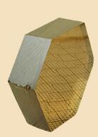
N-type Bulk GaN wafer 4'',Prime/LD grade
4'' Bulk GaN substrate wafer,HVPE Method
Diameter: 100.0±0.25mm
Orien: C-Plane(0001) ±0.5 deg
Primary flat orien:A-plane(11-20) ±0.2deg
Primary flat length: 32.5±2.5mm
Secondary flat orien:M-plane(10-10) ±0.2deg
Secondary flat length: 16.0±1.0mm
Thickness: 400±30um
TTV: </=15um ; Bow: </=20um
Micro-roughness: Ra</=0.2nm
Front surface finish: Epi-polished
Back surface finish: Polished
Micro-roughness: Ra</=1.0nm
Dislocation density: <(1~6)E6/cm2
Conduction type: N-type
Resistivity: ≤ 0.5 Ohm.cm
Laser Marking: Front side/Back side or None
Packaging: Clean room,indicidual fluoroware wafer vacuum sealed