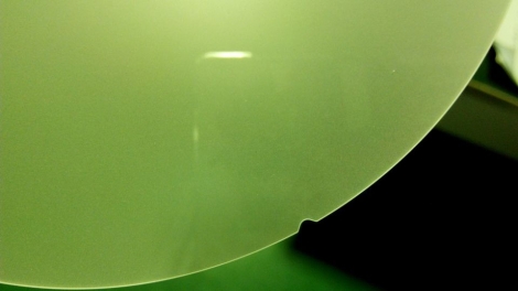
Standard spec. 8 inch sapphire substrate wafer
8'' C-plane Sapphire substrate wafer for GaN epitaxial growth
High Purity(>99.996%)and Monocrystaline Al2O3
Surface orien: C-plane<0001> Off-axis 0.35 +/- 0.15deg towards M-axis<10-10>
Notch orien: A-axis<11-20> +/- 0.3°
Notch Depth: 1.0 + 0.25/-0.00 mm/Notch per SEMI M1-1105
Notch Angle: 90 +5°/-1 °
Diameter: 200.0+/-0.25mm
Thickness: 0.725+/-0.025mm
Front side surface: Epi-polished,Ra</=0.3nm
Back side surface: Epi-polished,Ra</=0.3nm
Wafer edge: Round chamfer/bevel
TTV: </=20um
BOW: </=30um
Laser Mark: Back side scribing or N/A
Appearance/Surface Quality: Free of foreign contaminations/materials,No Scratch,Crack,Pores,Twins
Packaging: Class 100 clean room,vacuum sealed per single cassette